
Table of Contents
- Overview of the System
- Hardware
- Challenges
- Modifications
- Instructions
- Control Signals
- Sample Programs
- References
The thought to build an 8-bit Simple as Possible Computer was borne out of a need to gain hands-on experience with Digital Logic.
While my undergraduate digital electronics lab sessions did cover the basics: logic gates, timers, state machines, among others, a holistic appreciation of these building blocks was unfortunately missing. And hence building the 8-bit SAP computer was a solution to this need.
The SAP computer is based on a design found in “Digital Electronics” by Albert Malvino and the kit was sourced from Ben Eater.
The choice to go with the kit rather than sourcing individual parts was out of convenience. It was one less step to worry about. Ben Eater also had instructional videos and as such, I was confident that the project did indeed work and any troubleshooting needed would be easy to diagnose. For a thorough treatise on the workings of the computer, check out Ben Eaters videos on the same, as well as the aforementioned Albert Malvino book.
Overview of the System

The computer consists of the following modules:
- Clock Module
- Memory Address Register Module
- 16×8 Random Access Memory Module
- Instruction Register Module
- Program Counter Module
- Register A Module
- Arithmetic Logic Unit Module
- Register B Module
- Output Module
- 8-bit Bus
- 4×7 Segment Display Module
- EEPROM to convert from binary to decimal for the output Module
- 2xEEPROMs to store the computer’s Microcode
I made a walkthrough video on the workings of the computer on my YouTube channel that is embedded below:
Hardware
Parts List
| Name | Type |
| NE555P | Timer |
| 74LS00 | Quad 2-Input NAND Gate |
| 74LS02 | Quad 2-Input NOR Gate |
| 74LS04 | Hex Inverter |
| 74LS08 | Quad 2-Input AND Gate |
| 74LS32 | Quad 2-Input OR Gate |
| 74LS86 | Quad 2-Input XOR Gate |
| 74LS107 | Dual JK Flip-Flop |
| 74LS138 | 3-to-8 Line Decoder/Demux |
| 74LS139 | 2-to-4 Line Decoder/Demux |
| 74LS157 | Quad 2-to-1 Line Selector |
| 74LS161 | 4-bit Binary Counter |
| 74LS173 | 4-bit D Register |
| 74LS189 | 64-bit (16 x 4 bits) Static RAM |
| 74LS245 | 8-bit Bus Transceiver |
| 74LS273 | 8-bit D Register |
| 74LS283 | 4-bit Binary Adder |
| 74HC595 | 8-bit Shift Register |
| 28C16 | 16 kb (2048 x 8 bits) EEPROM |
Modules
Clock

The clock module is used to provide a clock signal to the various registers in the computer. It provides both a non-inverted clock signal and an inverted one. It is made up of:
- Chips
- 3 x NE555P Timers
- one 555 timer operates in astable mode. this is the clock signal used under normal operation of the computer
- another operates in monostable mode. this mode is used to single step through the computer’s operations especially when troubleshooting.
- the final one operates in bistable mode. this is used as a debouncing circuit for the momentary push button
- 1 x 74LS04 Hex Inverter: used as part of the logic to halt the computer and also to provide an inverted clock signal
- 1 x 74LS08 AND Gate
- 1 x 74LS32 OR Gate
- 3 x NE555P Timers
- Inputs
- 1 x Momentary Pushbutton: used for when single stepping the clock
- 1 x Slide Switch: used to select between the astable clock and monostable clock pulses
- 1 x 1 Mega Ohm Potentiometer: used to vary clock frequency from a couple
- Outputs
- The normal clock signal
- An inverted clock signal
- LEDs
- One blue LED is used to show the normal clock signal
- Another blue LED is used to show the inverted clock signal (this is connected closer to the Instruction Register)
- Control Signals
- HLT: halts the clock
Memory Address Register (MAR)

The Memory Address Register is used to select a specific memory when either data needs to be read from it or read from it. It consists of:
- Chips
- 1 x 74LS157 2:1 Line Selector: used to select whether the memory address bits will be provided by the bus or the 4-position DIP switch
- 1 x 74LS173 4-bit D Register: stores the 4 least significant bits from the bus that will be the address of a memory location in the RAM.
- Inputs
- 1 x 4-position DIP Switch: used a user input memory address when programming the computer
- 1 x Slide Switch: used to select whether the 74LS157 selector chip will output the user address from the 4-position DIP switch, or get the address from the bus through the 74LS173 chip.
- Outputs
- 4-bit Address: this address is used to access a memory location in the 16×8 RAM
- LEDs
- 4 x Yellow LEDs: used to show the memory address being accessed
- Control Signals
- MI: activates the 74LS173 chip to read the 4 LSBs from the bus
Random Access Memory

The Random Access Memory has 16 memory locations that can store 8-bit values. It is used to store the instructions and the program data needed by the computer. It consists of:
- Chips
- 1 x 74LS00 Quad NAND Gate: used as part of the logic that reads data from the bus into the RAM, it is activated by the RI signal
- 2 x 74LS04 Hex Inverter: used to invert the output of the 74LS189 to obtain the noninverted stored data.
- 3 x 74LS157 2:1 Line Selector:
- two are used to select between user programmed data entered using the 8-position DIP switch or data from the bus
- one is used to select whether user data will be written to the RAM using the write push button, or data will be written from the bus using the computer clock signal
- 2 x 74LS189 64-bit RAM: used to store instructions or data the computer needs to operate. It’s output is the inverted bits stored.
- 1 x 74LS245: used as the 8-bit transceiver to either read data from the bus or output data to the bus
- Inputs
- 4-bit Address from MAR: sets the address to which data is to be read from or written to the RAM
- 1 x 8-position DIP Switch: used to input data from the user
- 1 x Momentary Pushbutton: used to write data input by the 8-position DIP switch into the RAM
- Outputs
- 8-bit Data: contains either program instruction or data that is feed into the bus for use by the computer
- LEDs
- 8 Red LEDs: used to display the data stored at a particular memory location in the RAM
- Control Signals
- RI: sets the RAM’s bus transceiver to read data from the bus to be written into a memory location in the RAM
- RO: sets the RAM’s bus transceiver to write data to the bus from the selected memory location in the RAM
Instruction Register

The instruction register handles the instructions being executed at a particular time in the computer. It consists of:
- Chips
- 2 x 74LS173 4-bit D Register: used to store instruction bits. the 4 MSB store the microcode opcode while the 4 LSB stores the memory address of data in the RAM to be operated on
- 1 x 74LS245 8-bit Bus Transceiver: used as the 8-bit transceiver to either read data from the bus or output data to the bus
- LEDs
- 4 Blue LEDs: usedto display microcode opcode
- 4 Yellow LEDs: used to display 4-bit Memory Address of data to be operated on
- Control Signals
- II: sets the instruction register’s bus transceiver to read data from the bus of the instruction to be executed
- IO: sets the instruction register’s bus transceiver to output the 4-bit Memory Address of data / instruction to be retrieved from the RAM
Program Counter

The program counter keeps track of the current instruction being executed and it is used to advance to the next instruction need. It consists of:
- Chips
- 1 x 74LS161 4-bit Binary Counter: used to keep count of the instruction being executed
- 1 x 74LS245 8-bit Bus Transceiver: used as the 8-bit transceiver to either read the next instruction from the bus or output the next instruction to the bus. Only the 4 LSBs are used
- LEDs
- 4 Green LEDs: shows the instruction count
- Control Signals
- CO: outputs the contents of the program counter to the bus
A-Register/Accumulator and B-Register
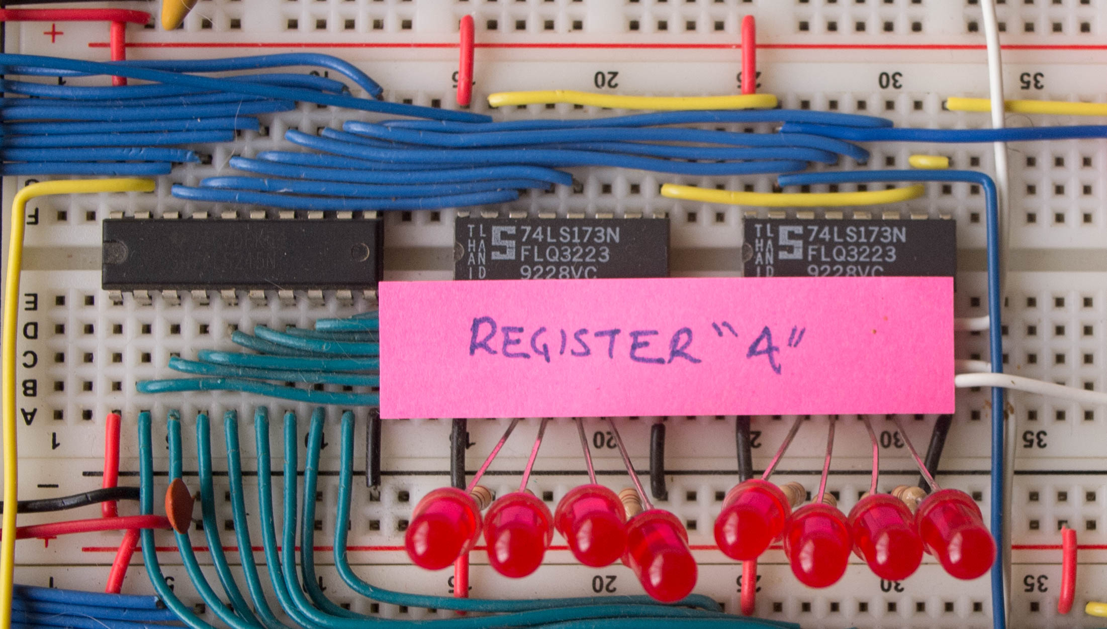
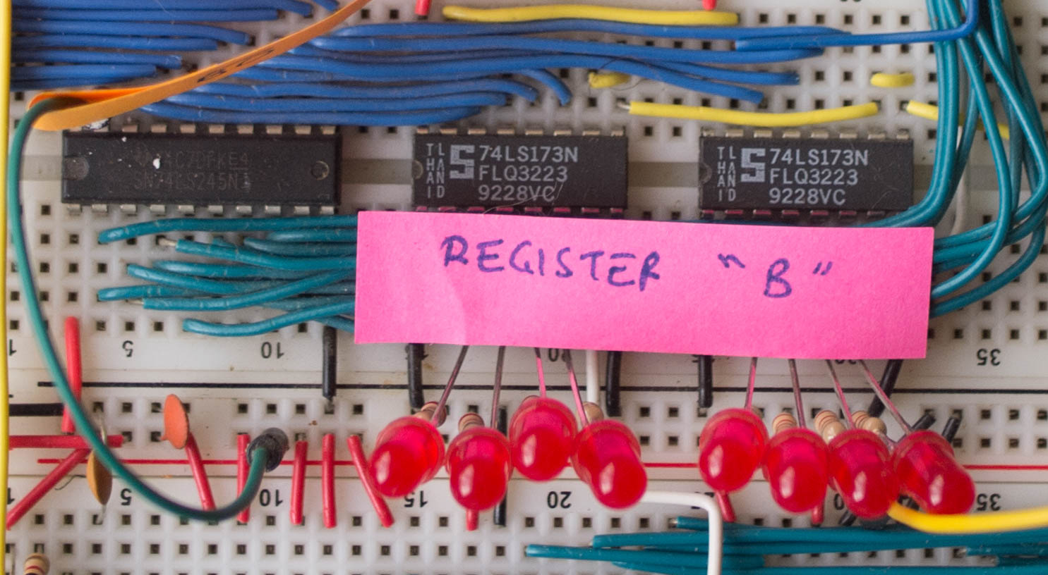
The A and B-registers are used to store data that is being operated on. The A-register additionally acts as the accumulator of that stores the results of a particular calculation. They are made up of:
- Chips
- 2 x 74LS173 4-bit D Register: used to store data bits that are to be used by the ALU in a calculation
- 1 x 74LS245 8-bit Bus Transceiver: used as the 8-bit transceiver to either read data from the bus or output data to the bus
- LEDs
- 8 Red LEDs: used to display the data in the Register
- Control Signals
- AI: sets the A register’s bus transceiver to read data from the bus
- AO: sets the A register’s bus transceiver to output data to the bus
- BI: sets the B register’s bus transceiver to read data from the bus
Arithmetic Logic Unit (ALU)

The arithmetic logic unit performs calculations on data that is held in the A and B registers. It can perform either addition or subtraction. For subtraction to be activated, the SU control signal must be high, otherwise, for addition, it must be low. The ALU consists of:
- Chips
- 2 x 74LS86 Quad XOR Gates: used to invert the value in the B register when it is set to subtract
- 1 x 74LS245 8-bit Bus Transceiver: used as the 8-bit transceiver to output data to the bus
- 2 x 74LS283 4-bit Binary Adder: used to add data from the A and B register
- LEDs
- 8 Red LEDs: used to display result of ALU operation
- Control Signals
- SU: sets the ALU to perform the subtraction “A-B”
- EO: outs the result of the ALU calculation onto the bus
Output

The output is used to display contents on the bus in decimal format when data is required to be output. It consists of:
- Chips
- NE555P: used as the independent clock for the output
- 1 x 74LS08: used for combining the clock signal with the control signal to decide when to store a value from the bus into the register as the register lacks an enable pin
- 1 x 74LS107: used as a 2-bit counter that increments on clock ticks
- 1 x 74LS139: used to convert the 2-bit counter into 4 separate lines to control the LEDs
- 1 x 74LS273: used to store the 8-bit value to be displayed
- 28C16: used to store the microcode to convert the binary value into digit segments to be used by the 7-Segment displays
- Outputs
- 4 x 7-Segment Displays: used to display binary value as a decimal value
- Control Signals
- OI: used to activate the output to read data from the bus and convert it to the corresponding decimal value.
Control Logic

The control logic is used to manage the control signals of the various registers of the computer. The instructions from the instruction register are fed into the EEPROMs which contain microcode that decode the instructions into a control signal word that is used to activate the necessary control signals to execute the desired instruction. Each instruction consists of a maximum of 5 microinstructions. The control logic consists of:
- Chips
- 1 x 74LS00: used as part of the logic used to RESET the computer registers
- 1 x 74LS138: used to indicate the microinstruction being executed
- 1 x 74LS161: used to count and keep track of the microinstruction step
- 2 x 28C16: used to store the instruction microcode
- Inputs
- Push button: used to reset the registers on the computer
- LEDs
- 3 Red LEDs: used to display the count of the microinstruction
- 5 Green LEDs: used to indicate the microinstruction being executed
- Control Signals
- All control signals are connected to the 2 control logic EEPROMs
Flags Register
The flags register is used to enable conditional jumps in the execution of the computer’s instructions. The conditional jumps are: jump on zero and jump on carry.
- Chips
- 1 x &74LS173: 4-bit register of which only two bits are used – one for Jump on Zero when the output of an ALU calculation is zero; and another for Jump on Carry, when the result of an ALU calculation is greater than 255
- LEDs
- 1 Green LED: used for the zero flag
- 1 Green LEd: used for the carry bit flag
Control Word

Control Word is used to indicate which control signals are active at any point in time during the computer’s operation
- 16 Blue LEDs: used to indicate which control signals are active
Bus

The bus is used to interconnect the various registers in the computer as described in the previous section.
- 8 Red LEDs: used to indicate the data that is present on the bus at given time
Instructions
Listed out below are the instructions that the 8-bit SAP breadboard computer can carry out.
| # | Mnemonic | Name | Opcode | Operand | Flags set | Flags read | Description |
| 0 | NOP | No operation | 0000 | Unused | Do nothing for a cycle | ||
| 1 | LDA | Load the accumulator | 0001 | Memory reference | Put the value of the referenced memory address into the A-register | ||
| 2 | ADD | Add | 0010 | Memory reference | CZ | Put the value of the referenced memory address into the B-register, and put the sum of A+B into the A-register | |
| 3 | SUB | Subtract | 0011 | Memory reference | CZ | Put the value of the referenced memory address into the B-register, and put the sum of A-B into the A-register | |
| 4 | STA | Store the accumulator | 0100 | Memory reference | Store the value of the A-register into the referenced memory address | ||
| 5 | LDI | Load immediate | 0101 | Value | Put the value from the operand into the A-register | ||
| 6 | JMP | Jump | 0110 | Memory reference | Jump to the instruction at the referenced memory address | ||
| 7 | JC | Jump if carry | 0111 | Memory reference | C | Jump to the instruction at the referenced memory address if the carry flag is set | |
| 8 | JZ | Jump if zero | 1000 | Memory reference | Z | Jump to the instruction at the referenced memory address if the zero flag is set | |
| 9 | OUT | Output | 1110 | Unused | Output the value of the A-register on the 7-segment display | ||
| 10 | HLT | Halt | 1111 | Unused | Halt the computer |
Control Signals
| Control Signal | Associated Module | Description |
| HLT | Clock | Halt the clock to halt the computer |
| MI | Memory Address Register | Memory address register in |
| RI | RAM | RAM data in |
| RO | RAM | RAM data out |
| IO | Instruction Register | Instruction register out |
| II | Instruction Register | Instruction register in |
| AI | A-Register | A register in |
| AO | A-Register | A register out |
| EO | ALU | ALU out |
| SU | ALU | ALU subtract |
| BI | B-Register | B register in |
| OI | Output Module | Output register in |
| CE | Program Counter | Program counter enable |
| CO | Program Counter | Program counter out |
| J | Program Counter | Jump (program counter in) |
| FI | Flags Register | Flags in |
Modifications
The most significant modification was adding resistors to all the LEDs. While the 74LS chips used did have internal resistors, this only guaranteed that the LEDs wouldn’t burn out, however, the LEDs still managed to draw quite a bit of power leading to a reduced voltage across the board. This reduced voltage meant that sometimes the threshold voltage for a logic 1 on the chips wasn’t being met, leading to inconsistency in the execution of the computer’s instructions. On recommendation from the Ben Eater Reddit page, I had to solder resistors onto the LED legs. This option was chosen to maintain the layout of the board without the need for extra space for the resistors.

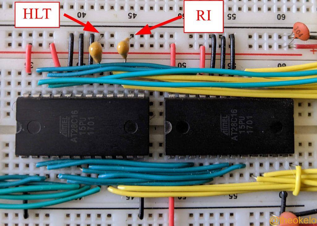
The EEPROMs hosting the computers instruction microcode did seem to behave unreliably with control signals that were not inverted i.e. the HLT, RI and OI. In the case of the HLT line, for instance, the computer tended to get reset when it wasn’t supposed to, and interfered with the program sequence/program data. A solution that ended up working was attaching a 1 μF capacitor between the said pins and ground to eliminate the unwanted triggers.
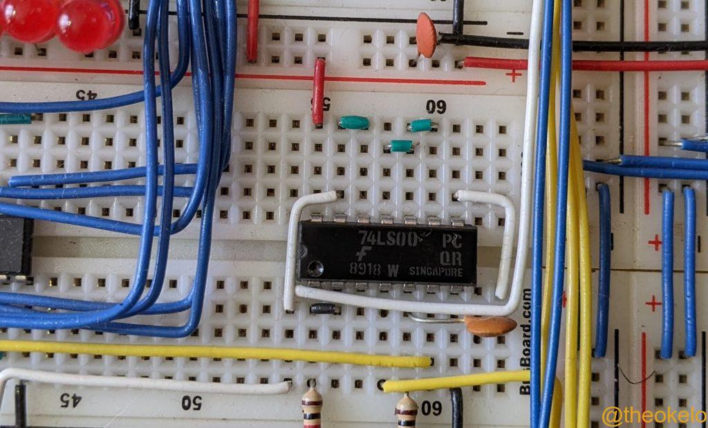
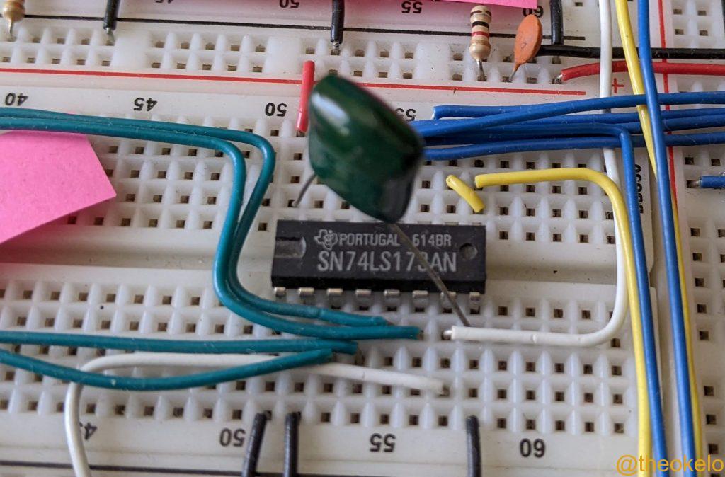
As part of the RAM circuit, the RI control signal was NANDed with the clock signal and a 0.01 μF capacitor was added to pull the output (that when to the RAM’s write line) low only at the instance that the clock signal when high. However, this RC circuit did create some resonance that travelled back through the clock wires creating noise that cause registers to latch when they weren’t supposed to. This was fixed by isolating the main clock line from the RC circuit on the NAND IC by using the unused NAND gate pins to create a buffer so there wouldn’t be any reflections back into the main clock line.
A 0.1 μF capacitor was placed across the Memory Address Register to eliminate noise on the line that would cause the register to reset unexpectedly.
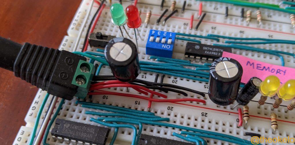
To improve voltage stability across the board, 0.1 μF capacitors were added across all the power rails to ensure a stable voltage distribution. Additionally, to ensure reliable power, the power barrel adapter was firmly attached to the board using multiple jumper wires. Multiple jumper wires were also used to ensure sufficient power delivery to the circuit. Two 470 μF capacitors were connected close to the supply power barrel to further reduce voltage fluctuations.
To read more in-depth on the above-mentioned issues and other’s that I did not mention you can check out Christian Ihle’s detailed documentation on the same
Challenges
The major challenge I faced in the build of the computer was when one of the 74LS189 RAM ICs couldn’t reliably hold data that was stored in it and had to be replaced. I couldn’t source the part locally and had to get it from AliExpress. Unfortunately, this was in the early days of the COVID-19 pandemic and there was an interruption in the postal courier services I relied on. What typically is a 2 to 4 week shipping time ended up being 17 weeks. This one is more of a supply chain problem rather than a technical one, but a major problem nonetheless.
Sample Programs
Fibonacci
One of the programs that I run on the 8-bit SAP is the Fibonacci Sequence. The Fibonacci sequence is the series of numbers: 0, 1, 1, 2, 3, 5, 8… whereby the next number is found by adding the two numbers before is.
The 8-bit SAP calculates the Fibonacci Sequence between 1 and 255 since the range of computer is [0,255]/[-127,127]. This program runs in a loop that is activated whenever the 256 carry bit of the ALU is activated.
| # | Instruction | Address | Memory | Content |
| 0 | LDI 1 | 0000 | 0101 0001 | Load the value 1 from the instruction register into the A-register |
| 1 | STA 14 | 0001 | 0100 1110 | Store the contents of the A-register in memory location 1110 |
| 2 | LDI 0 | 0010 | 0101 0000 | Load the value 0 from the instruction register into the A-register |
| 3 | STA 15 | 0011 | 0100 1111 | Store the contents of the A-register in memory location 1111 |
| 4 | OUT | 0100 | 1110 0000 | Output the contents of the A-register |
| 5 | LDA 14 | 0101 | 0001 1110 | Load the contents of memory location 1110 into the A-register |
| 6 | ADD 15 | 0110 | 0010 1111 | Load the contents of memory location 1111 into the B-register, then add the contents of the B-register to the A-register |
| 7 | STA 14 | 0111 | 0100 1110 | Store the contents of the A-register into memory location 1110 |
| 8 | OUT | 1000 | 1110 0000 | Output the contents of the A-register |
| 9 | LDA 15 | 1001 | 0001 1111 | Load the contents of memory location 1111 into the A-register |
| 10 | ADD 14 | 1010 | 0010 1110 | Load the contents of memory location 1110 into the B-register, then add the contents of the B-register to the A-register |
| 11 | JC 0 | 1011 | 0111 0000 | Jump to memory location 0000 if the ALU carry bit flag is on i.e. it is past 255 |
| 12 | JMP 3 | 1100 | 0110 0011 | Jump to memory location 0011 |
| 13 | – | 1101 | – | Not used |
| 14 | X Variable | 1110 | Stores the X variable | |
| 15 | Y Variable | 1111 | Stores the Y variable |
References
- Build an 8-bit Computer from Scratch – Ben Eater
- A. P. Malvino and J. Brown, Digital Computer Electronics. London, England: McGraw-Hill Education (ISE Editions), 1992.
- 8-bit Computer Documentation on Christian Ihle’s Github
- What I Have Learned (a master list of what to do and what not to do)
Nice documentation, can you make a video on building it?
Thank you.
Hi, is it possible to ask for the copy of schematic diagram. Thank you.
Fantastic documentation. I just ordered a kit and will come back to your site to guide me through together with Ben Eaters Video and the Reddit forum. I am a complete novice, but with so much excellent help it seems doable. All the best!
Could you show your codes in C language? I want to try by myself.
Great to see this! It’s so well documented that others will be very inspired to learn from it.
Thanks, that’s part of my inspiration too, that more people will come across it and get interested in digital electronics and computers in general.