One of the circuits that I’ve spent an inordinate amount of time investigating this year is the Analogue Multiplier.
An analogue multiplier is a circuit block which takes two analogue signals and produces an output which is proportional to their product.
Analogue multipliers can be integrated as part of a larger circuit blocks to perform specific analogue computation such as: modulation, multiplication, squaring, division, square-root generation, mean-square calculation.
For the purposes of this exercise, let’s consider an Analogue Multiplier as an analogue modulator.
Now the basics of modulation is that you typically have one waveform, the modulating signal, that contains information that you want to use to modulate a carrier signal, often of a much higher frequency, so that you can transmit your message over vast distances.
Assuming we have two sinusoidal signals: a = cos(x) (modulating signal) and b = cos(20x) (carrier signal) an analogue multiplier would produce the output signal c = cos(x)cos(20x) as illustrated in the graphs below:


Just a Little Bit of Theory
Multipliers can be categorised as: one quadrant, two quadrant or four quadrant depending on the nature of the respective inputs as listed below:
- one quadrant – the polarity of a and b must both be the same i.e. both are +ve or both are -ve
- two quadrant – the polarity of one of the signals e.g. a, must strictly be held constant at either +ve polarity or -ve polarity, while the other signal, b in this case, can vary
- four quadrant – the polarity of both a and b can vary
The quadrant within which a specific multiplier operates is dependent on how you build your circuit.
Analogue multipliers can be built using transistors, or op amps; each with its own advantages and disadvantages.
For the purpose of this post, I’ll be focusing on transconductance analogue multiplier. This first part will deal with a two quadrant multiplier, and a second part will deal a four quadrant multipliers.
The Building Blocks of the 2 Quadrant Analogue Multiplier
A two quadrant analogue multiplier can be achieved by building a transistor circuit that utilises a differential pair and a current mirror.
Taking the emitter coupled pair shown above, the currents Ic1 and Ic2 are given by:
$$I_{c1} = \frac{I_{EE}}{1+exp\left(-\frac{V_{id}}{V_T}\right)}$$
$$I_{c2} = \frac{I_{EE}}{1+exp\left(\frac{V_{id}}{V_T}\right)}$$
If output is taken between the collectors of Q1 and Q2 the differential current is:
$$\Delta I_{c}=I_{c1}-I_{c2}=I_{EE} \tanh{\left(\frac{V_{id}}{2V_T}\right)}$$
Plotting this equation we come to our first limitation of this implementation, as long as the value of Vid is small, we can operate within the linear region of the I-V curve
Thus, tanh can be approximated as:
$$\tanh{\left(\frac{V_{id}}{2V_T}\right)} \approx \frac{V_{id}}{2V_T} \hspace{10 mm}\frac{V_{id}}{2V_T} \ll 1$$
And the differential output current can be written as:
$$\Delta I_c\approx I_{EE}\left(\frac{V_{id}}{2V_T}\right)$$
IEE, which is the bias current for the emitter-coupled pair can be made proportional to a second input signal, Vi2.
Thus from the current mirror circuit
$$I_{EE}\approx K_o(V_{i2}-V_{BE(on)})$$
Thus the differential output current of the emitter-coupled pair can be calculated as:
$$\Delta I_c=\frac{K_o V_{id}(V_{i2}-V_{BE(on)})}{2V_T}$$
As per the opening definition of an analogue multiplier, we’d be multiplying the signals Vid and Vi2 but while working under some constraints:
- Vid is small (in the mV range)
- Vi2 is greater than VBE(on) (a DC offset would be needed). It is this restriction that makes the circuit a two quadrant multiplier.
Armed with this theoretical background a practical circuit can be implemented.
The Circuit
Parts List:
- 4 x 2N3904 Transistors (BC337 could also be used)
- 2 x 1 k Resistors
- 1 x 470 k Resistor
- Function Generator with dual outputs and DC Offset Functionality
- Power Supply
- Oscilloscope
- Breadboard
- Jumper Cables
The test circuit to be constructed is illustrated below:
Simulating the circuit, we get to see the waveforms that we shall expect to obtain:

The first waveform in blue will be our Vi2, the modulating signal which will have an amplitude of 5 V with a frequency of 5 kHz and a DC offset of 5 V so that Vi2 > VBE(ON).
The second waveform in yellow will be our Vid which is fed into the differential pair as our carrier signal with an amplitude of 100 mV at 100 kHz. The 100 mV signal is chosen so that the differential pair is operating within its linear region.
And finally we have the output signal which is taken as the differential between the collectors of Q1 and Q2.
The Practical Build
With our theory that has been validated by simulation it’s time to build the circuit. For this there are a couple of things to note.
First, I’d advise that the transistors be as closely matched as possible, probably by getting transistors from the same batch (brand new transistors are the best option). Test the transistors to be sure that they are working; faulty transistors can be a major source of errors when working with transistor circuits. For BJT transistors a quick check can be done by performing a diode/short circuit test on the Collect-Base and Base-Emitter Junctions.


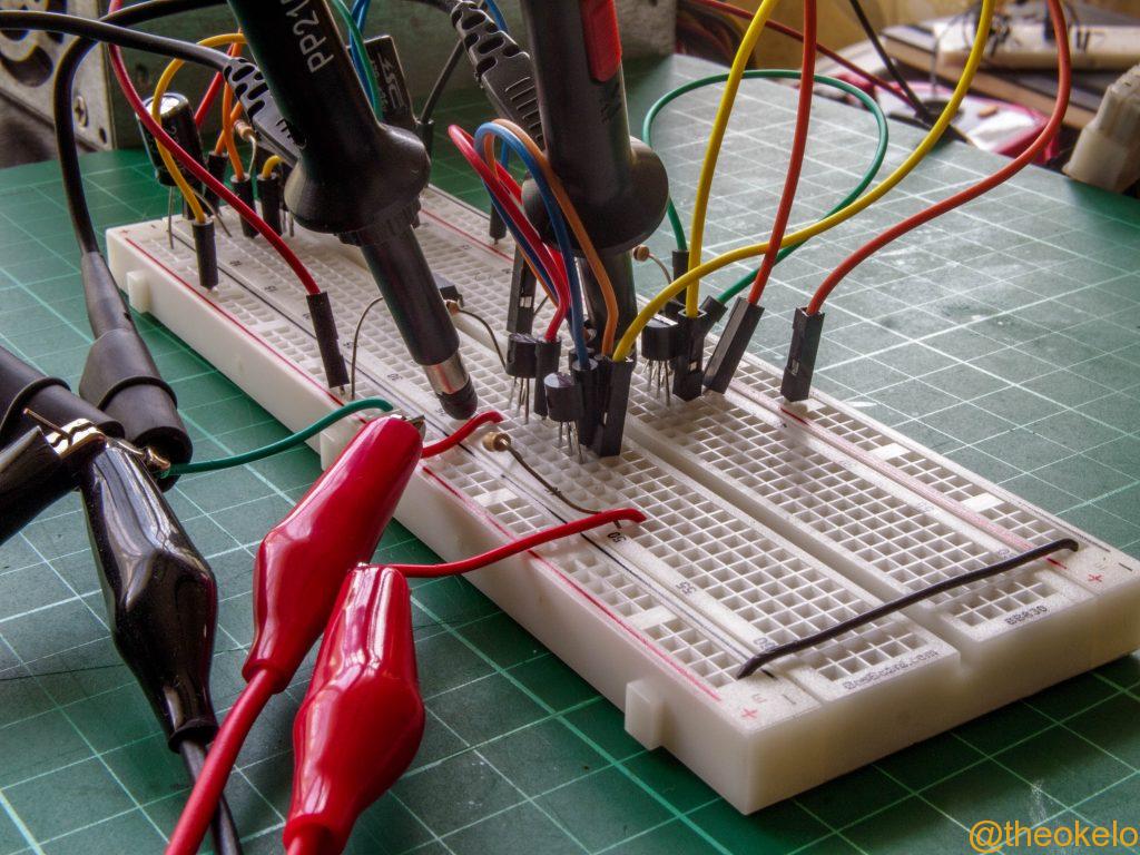
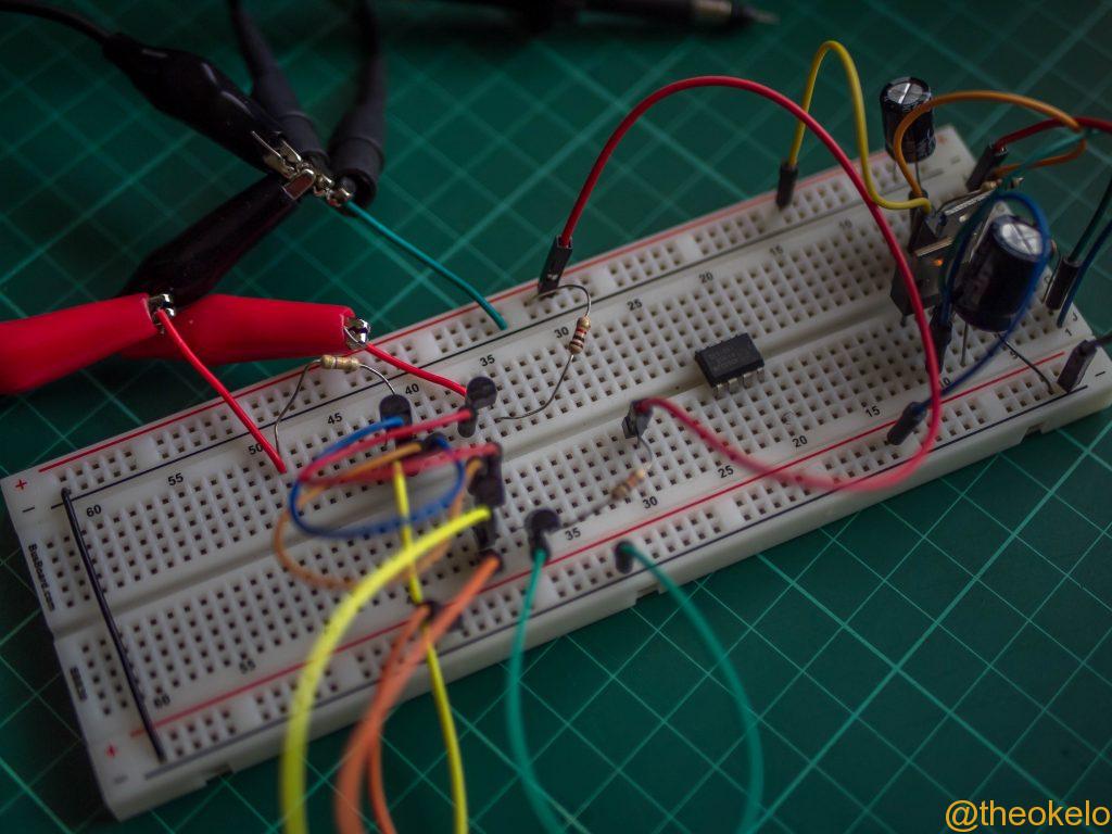
Second, try as much as possible to get a low noise power supply. Unfortunately for me my power supply is a noisy ATX power supply so I’m using a filtering circuit (that’s what those capacitors on the right side of the second photo are) to try and get as best a performance as I can. Noise is very critical to the success of your implementation considering one of the signals has to be in the millivolts range and power supply ripple can throw your expected signals off balance.
With that the execution should go as illustrated below:


The waveforms obtained are as follows:
- a) is the “carrier signal” with an amplitude of 50 mV at 100 kHz
- b) is the “modulating signal” with an amplitude of 5 V at 5 kHz with a DC offset of +5 V
- c) is signals a) and b) on the same screen
- d) is the outputs from the collector’s of Q1 and Q2 respectively
- e) is d) plus the differential output i.e. $V_{CQ1}-V_{CQ2}$ sandwiched between them
Going by e) we were able to build a circuit that multiplied two input signals and gave an output that was proportional to their product


So that’s one way to build a two quadrant multiplier using transistors. Typically, two quadrant multipliers are not used in practical implementations of multipliers as they are extremely limiting especially in the area of communication. Furthermore the restriction that Vid be limited to small values is a major disadvantage. Thus a much better implementation of multipliers is for it to operate as a four quadrant multiplier, which the Gilbert Cell is a prime choice. But more on that later.
References
- P. Gray, P. Hurst, S. Lewis and R. Meyer, Analysis and design of analog integrated circuits, 5th ed. New York: Wiley, 2009, pp. 704-706
- A. Grebene, Bipolar and mos analog integrated circuit design. New Jersey: Wiley-Interscience, 2003, pp. 451-457
Great article!